ABSTRACT
Manipulation of single cells and particles is important to biology and nanotechnology. Our electrokinetic (EK) tweezers manipulate objects in simple microfluidic devices using gentle fluid and electric forces under vision-based feedback control. In this dissertation, I detail a user-friendly implementation of EK tweezers that allows users to select, position, and assemble cells and nanoparticles.
This EK system was used to measure attachment forces between living breast cancer cells, trap single quantum dots with 45 nm accuracy, build nanophotonic circuits, and scan optical properties of nanowires. With a novel multi layer microfluidic device, EK was also used to guide single microspheres along complex 3D trajectories. The schemes, software, and methods developed here can be used in many settings to precisely manipulate most visible objects, assemble objects into useful structures, and improve the function of lab-on-a-chip microfluidic systems.
PRINCIPLES OF ELECTROKINETIC TWEEZING
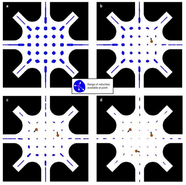
Fig. 2 Velocities available for control
As long as there are more electrodes than components of velocity to control, there are many possible solutions to the control problem. However, some solutions require high voltages that are impossible to create in practice. Here are shown the velocities it is possible to create to control the 1st, 2nd, 3rd, and 4th object (a, b, c, and d). Around each grid point (magenta), a region (blue) is drawn in which it is possible to achieve the control velocity for each additional object. a)
The first object can be easily controlled in any direction anywhere in the control region. b-c) As the number of controlled objects increases, the range of velocities available for the next one decreases, especially in the vicinity of the objects. d) Control of 3 objects consumes most of the available velocity, despite there being two more electrodes than components of velocity to control.
IMPLEMENTATION OF ELECTROKINETIC TWEEZING
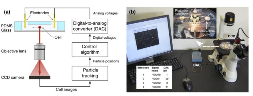
Fig. 3 Schematic of the experimental setup
(a) A CCD camera images the cells in bright-field or fluorescence illumination. A cell-tracking algorithm computes the position of the chosen cell and a control algorithm then determines the needed actuation voltages which are applied through a digital-to-analog converter (DAC) and platinum electrodes to the microfluidic device.
(b) Photograph of the experimental setup with zoomed view of a microfluidic device. Here the yellow round shapes are the four reservoirs, platinum wire electrodes are brought in contact with the cell buffer fluid in these reservoirs. Left corner: The connection table for connecting the electrodes with the DAC (Measurement Computing USB-3101).
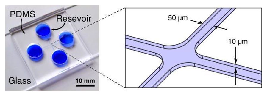
Fig. 4 Microfluidic control device for one object
The microfluidic device (left) consists of two intersecting microchannels each ~2 cm long made from PDMS using standard soft lithography techniques. Each channel is 10 µm deep and 300 µm wide except at the intersection (right), where it is narrows to a width of 50 µm to concentrate electrokinetic forces.
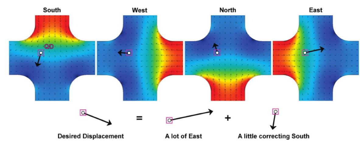
Fig. 5 Model of the four flow modes resulting from voltages applied to each electrode
Any desired correcting velocity, at any particle location, can be created by combining these four actuation modes. Black arrows show the microfluidic velocities, color shows the applied electric potential, and the enlarged black arrows show an example of velocity decomposition.
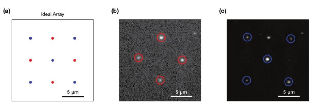
Fig. 13 Array of preselected QDs
(a) Idealized array design with the two different types of QDs alternating in a checkerboard pattern. (b) Completed array as visualized through a bandpass filter centered at 710 nm. The four QDs emitting at ~705 nm are circled in red while the 655 nm emitting QDs are not visible. (c) The same completed array as visualized through the 655 nm band-pass filter. The QDs emitting at 655 nm are circled in blue.
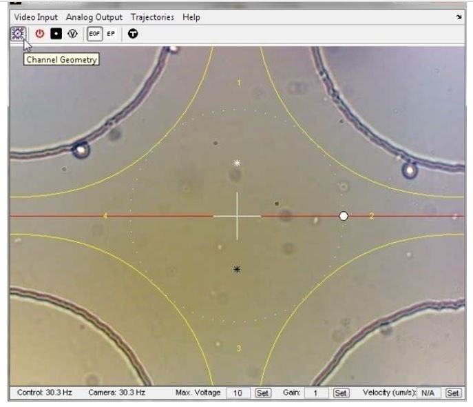
Fig. 7 Graphical user interface (GUI) and coordinate calibration
This simple GUI allows users to select objects, drag them by mouse, draw trajectories for objects to follow, and record experiments. To properly transform between the coordinates used for image processing and those used for control calculations, a schematic of the control device must be dragged, rotated, and scaled to match the image.
NANOWIRE ASSEMBLY
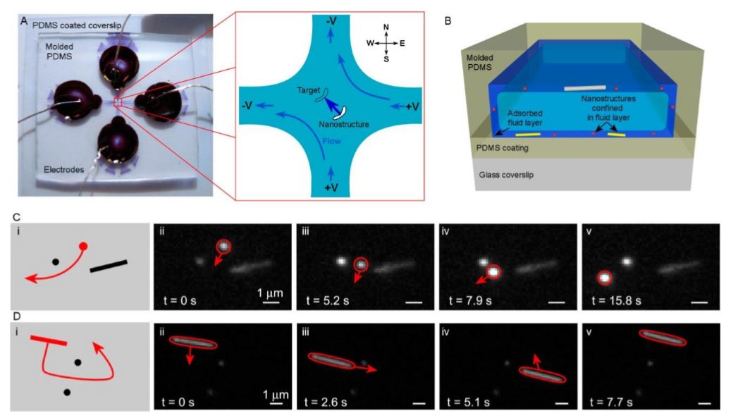
Fig. 14 Electrokinetic control of nanostructures
(a) Optical image of the microfluidic device. Channels are formed from molded PDMS placed on top of a PDMS-coated coverslip. Reservoirs are cut from the PDMS to access the channels (here filled with a dark fluid). Electrodes placed in the reservoirs actuate electroosmosis. The expanded region corresponds to the control chamber in the center of the cross channel. Voltages applied to the four electrodes create electroosmotic flow to move a nanostructure in any desired direction within the control chamber.
(b) Schematic side view of the microfluidic channel depicting the fluid layers that confine nanostructures to the device surfaces. The microfluidic device is 5 μm high and the fluid layer is approximately 100 nm thick. (c) )i) Schematic of quantum dot steering between two nanostructures adhered to the device surface. (ii–v) Time-stamped images of the steering process. Arrows denote the direction of fluid flow. (d) (i) Schematic of silver nanowire steering between two nanostructures on the surface. (ii–v) Time-stamped images of the steering process. Arrows denote direction of fluid flow.
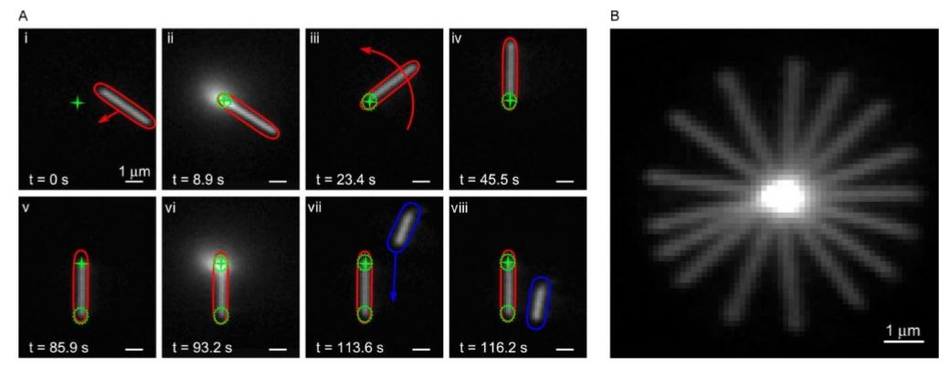
Fig. 17 Orienting a silver nanowire after immobilizing one of its ends
(a) (i) The nanowire is positioned so that its end is at the focus (green cross hair) of the UV laser. (ii) Local UV exposure immobilizes one end of the nanowire. (iii,iv) The nanowire is rotated about the immobilized end and held at a vertical orientation. (v) The stage is translated so that the UV focus is at the free end of the nanowire. (vi) A second UV exposure immobilizes the second end of the nanowire. (vii,viii) Subsequent actuation of fluid flow confirms that the nanowire is immobilized, as is seen from the motion of a second silver nanowire (blue). (b) Composite image from several frames of a silver nanowire rotating 360° about its immobilized end.
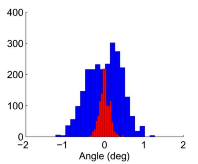
Fig. 18 Histograms comparing the measured angle of a silver nanowire that is immobilized on a surface (red) with one that is oriented by flow control (blue)
Affixing one end of a silver nanowire to the surface with polymer provides precise control of the nanowire’s orientation. We quantify orientational precision by monitoring the angle of a wire held by feedback for 1 minute. Fig. 18 plots histograms of the measured angles for the held wire (blue) compared to the measured angle for an immobile silver nanowire (red).
NANOSCALE IMAGING AND SPONTANEOUS EMISSION CONTROL
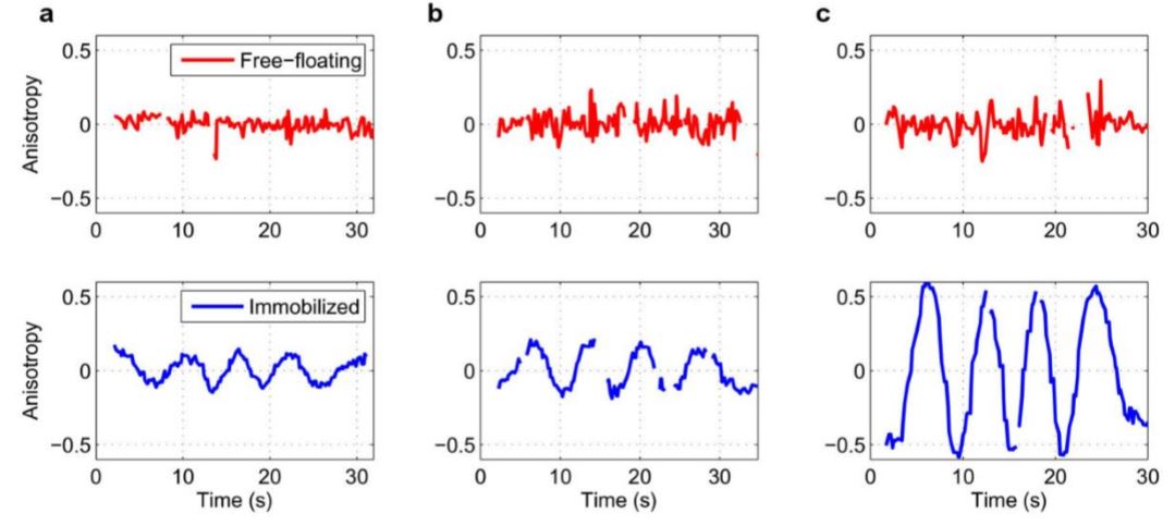
Fig. 22 QD Polarization in channel
The emission anisotropy of three pairs of QDs (a-c) measured as a function of polarization (which was rotated in time). Each pair consisted of a free-floating (red) and an immobilized (blue) QD. The emission polarizations for each pair were characterized simultaneously using a setup where the emission was sent through a half-wave plate and then split into vertical (V) and horizontal (H) polarization by a calcite beam displacer.
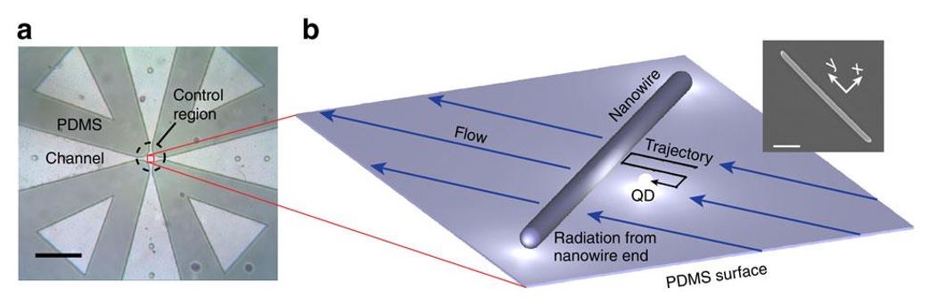
Fig. 23 Near-field probing with a single QD
(a) Optical image of the microfluidic crossed-channel device. Flow in the center control region (dashed circle) is manipulated in two dimensions by four external electrodes (not shown). Scale bar, 500 μm. (b) Schematic of the positioning and imaging technique. A single QD is driven along a trajectory close to the wire by flow control. The coupling between the QD and AgNW is measured either by the radiated intensity from the wire ends or by QD lifetime measurements. The inset shows a scanning electron microscopy image of a typical AgNW used in our experiments (scale bar, 1 μm). The – coordinate system is defined relative to the orientation of the AgNW, as illustrated in the inset.
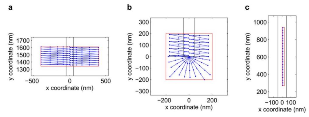
Fig. 26 Scanning Trajectories
(a) Mid-wire scanning trajectory corresponding to Fig. 27. (b) A trajectory scanning the wire tip corresponding to Fig. 30. (c) A trajectory scanning the wire along the side corresponding to Fig. 32. Blue points connected with lines correspond to the trajectory points, connected in order of scanning. During the experiment, flow is applied to position the QD to the desired trajectory point for two seconds before moving on to the next point. Red boxes define the scanning regions.
Black lines designate the physical extent of the wire. Some points along the trajectory lie inside the wire or on the opposite side of the wire, however, since the wire acts as an obstacle the QD cannot generally reach these points and instead is forced against the wire to ensure data is collected as close as possible to the surface. Additionally, the trajectory points are more densely spaced closer to the wire in order to ensure probing of the near-field region.
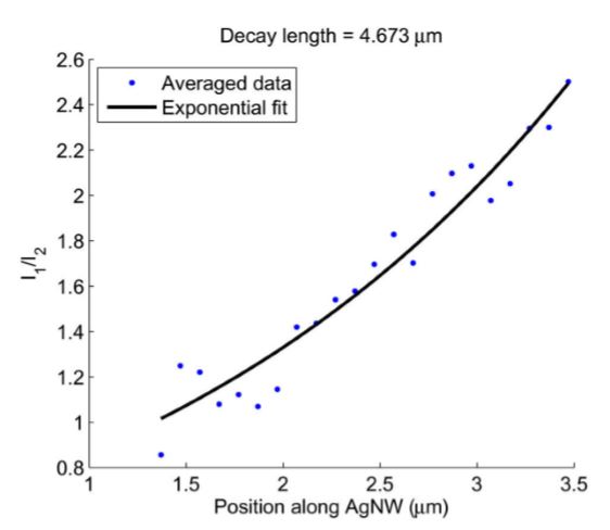
Fig. 28 SPP decay along AgNW length
Ratio of emission intensity measured from both AgNW ends as a function of position along the wire. The black line is an exponential fit.
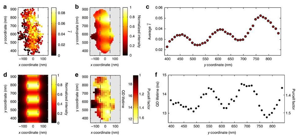
Fig. 32 SPP wave interference along an AgNW
(a) Scatter plot of the measured QD positions near the end of the wire. The color of each data point corresponds to the value of measured at each location. The dashed region indicates the location of the AgNW. (b) Reconstructed image using a Gaussian-weighted average. The image intensity is normalized by its maximum. (c) Plot of an averaged value of as a function of position along the wire.
(d) FDTD simulation of the field intensity standing-wave pattern along the side of the AgNW (normalized by its maximum), with the profile within the dashed wire region corresponding to the field immediately outside the wire. (e) Image of the measured QD lifetime as a function of position. The color scale is labeled with both lifetime and Purcell factor. (f) Plot of QD lifetime measured along the length of the AgNW.
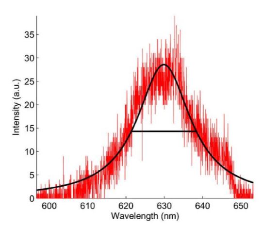
Fig. 33 Single QD Spectrum
Emission spectrum (red) of a single QD that was immobilized on a glass coverslip as measured using a grating spectrometer (Acton SP 2758). The black curve is a Lorentzian fit indicating a spectral linewidth of 17 nm.
ELECTROKINETIC TWEEZING IN 3D

Fig. 34 Schematic of vision-based electrokinetic feedback control in two dimensions
The system is shown manipulating a neutral particle with electroosmotic (EO) flow only. A microfluidic device, control algorithm, and particle tracking system are connected in a real-time feedback loop. The vision tracking system measures the position of a particle chosen by a user. The control algorithm then calculates which EO fluid flow will carry this particle from its current towards its desired position, and electrodes then actuate the necessary fluid flow. This feedback loop repeats continually and at each time moves the chosen particle closer to its desired position, thus either trapping it in place or steering it along any desired trajectory.
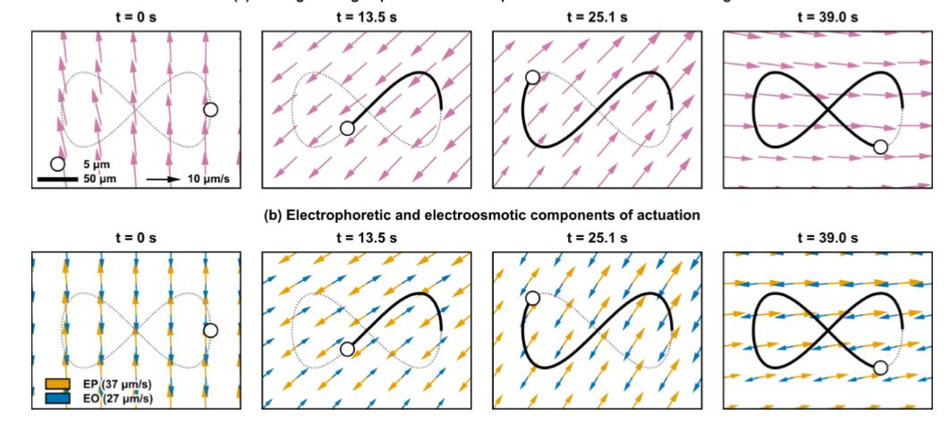
Fig. 39 Electrokinetic velocities created while steering a particle along a vertical trajectory
(a) By applying the correct voltage to each of the eight electrodes at once it is possible to impart the desired horizontal and vertical EK velocities to a particle at any location. For example, here we show the EK velocity fields created while steering a particle along the vertical ∞ trajectory shown in panel (b) of Fig. 35. Note that at each time the EK velocity is pointed along the tangent of the desired trajectory at the location of the particle (black circle). (b) For a negatively charged particle, the velocity components due to EP (orange) and EO (blue) oppose each other, but since their sum is usually non-zero the control algorithm can use their combination (the magenta arrows in panel a) to manipulate any single particle as desired.
CONCLUSIONS
In this thesis I described the implementation of a system that manipulates nano and microscopic objects using electrokinetic forces, its use in manipulating cancer cells and nanoparticles, and its extension into three dimensions. EK tweezers are a vision-based feedback control system that allow simple microfluidic devices to perform complex laboratory techniques and uses forces that scale favorably for small objects, enabling gentle control of cells and nanoprecise control of nanoscale objects. The implementation of EK tweezers uses commercially available hardware and software and provides an easy-to-use graphical user interface, making it easy adapt to multiple research applications
. As a demonstration, EK tweezers are used to measure the attachment forces between two cancer cells that possess microtentacles, protrusions from the cell membrane present on circulating tumor cells (CTCs) that allow them to attach reattach at distant tissues and to other CTCs, leading to metastasis. EK tweezers are next used to manipulate nanoscopic quantum dots and metallic nanowires for on-demand selection, assembly, and imaging of nanophotonic structures. Quantum dots (QDs) are semiconductor nanocrystals that can be used as single-photon emitters146 when placed with 150 nm of the high field regions of nanophotonic circuits.
Using sensitive optics and a high viscosity fluid, single QDs were trapped with an accuracy of 45 nm and steered on complex trajectories with an accuracy of 120 nm, well within the desired accuracy. A photoresist was added to the fluid, allowing QDs to be immobilized in a polymer with 127 nm accuracy when exposed to a UV flash. Metallic nanowires allow light to be transferred in the form of surface plasmons and can be used to construct nanophotonic circuits such as sub wavelength interferometers158 resonators,180 single-photon sources,and nonlinear quantum devices. EK tweezers positioned and oriented silver nanowires by pivoting them around polymerized anchors, and assembled them into complex nanostructures. The optical properties of single nanowires were then imaged with nanoscale resolution by scanning single QD probes in around them using a program run in parallel to control.
Source: University of Maryland
Author: Zachary Cummins