ABSTRACT
To allow fast communication—at several Gb/s—of multimedia content among processors and memories in a multi-processor system-on-chip, a new approach is emerging in literature: Wireless Network-on-Chip (WiNoC). With reference to this scenario, this paper presents the design of the key element of the WiNoC: the antenna. Specifically, a bow-tie antenna is proposed, which operates at mm-waves and can be implemented on-chip using the top metal layer of a conventional silicon CMOS (Complementary Metal Oxide Semiconductor) technology.
The antenna performance is discussed in the paper and is compared to the state-of-the-art, including the zig-zag antenna topology that is typically used in literature as a reference for WiNoC. The proposed bow-tie antenna design for WiNoC stands out for its good trade-off among bandwidth, gain, size and beamwidth vs. the state-of-the-art.
DESIGN OF THE ON-CHIP HIGH-BANDWIDTH ANTENNA
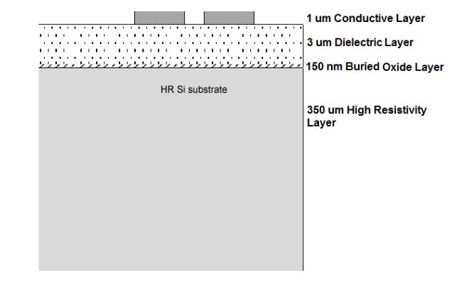
Figure 2. Side view (in the case of a Co-planar Stripline (CPS) implementation) of the adopted single-chip multi-layer structure
Figure 2 shows a side view of the multi-layer structure in the example case of the CPS implementation. For the sake of space, the figure is not to scale, since the height of the high resistivity layer is two orders of magnitude higher than the height of the conductive and dielectric layers, and three orders of magnitude higher than the height of the buried oxide layer.
ANTENNA CHARACTERIZATION
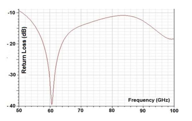
Figure 4. Return loss of the antenna as a function of frequency
At 60 GHz, the performance in terms of S-parameters has a maximum gain (from CST simulations) of about −7 dBi and a return loss of −39.5 dB. The percentage radiation efficiency η is about 20%. In the state-of-the-art, the antenna bandwidth capability is calculated as the frequency range where the return loss parameter is below −10 dB. Figure 4 shows the S11 antenna performance vs. frequency.
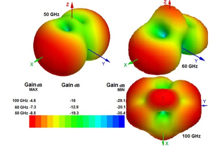
Figure 5. Radiation pattern and antenna gain at 50 GHz, 60 GHz, 100 GHz
Frequency values above 100 GHz are not taken into account in this work, since above 100 GHz the CMOS technology is not a suited technology for the integration of the transceivers. Indeed, above 100 GHz, the gain values of the low noise amplifier (LNA) and of the power amplifier (PA) will be too low, and the receiver noise figure (NF) will be too high. Figure 5 shows the 3D radiation pattern and the antenna gain as a function of frequency, at 50 GHz, 60 GHz and 100 GHz, considering a direction of 0 degrees in the X–Y plane in Figure 3.
COMPARISON OF THE DESIGNED ANTENNA VS. THE STATE-OF-THE-ART
With respect to antennas in the sub-10 GHz domain, the area occupation of the antenna design in Section 3 is limited to about 0.6 mm2. This size is compliant with integration on a single-chip. On the contrary, the size of the antennas proposed in Ref is orders of magnitude higher than the on-chip bow-tie antenna in this work.
IMPACT OF THE PROPOSED ANTENNA ON THE NOC INFRASTRUCTURE PERFORMANCE
This section evaluates the impact of the proposed antenna on the performance of the whole NoC infrastructure, and hence on the performance of an MPSoC, with respect to the use of a zig-zag antenna. It is worth noting that the higher HPBW of our design vs. zig-zag antenna leads to a larger number of cores that can be reached by the WiNoC.
CONCLUSIONS
The design of a mm-wave antenna for wideband wireless communications on-chip, WiNoC, is presented in this work. WiNoC is an emerging trend in on-chip communications to solve power consumption and latency issues of conventional metal-wires in the case of links above 1 cm in size (e.g., distant tiles in a multi-processor system-on-chip). The aim is to interconnect multiple macrocells of homogenous or heterogeneous MPSoCs. The proposed bow-tie antenna design has been characterized in the range from 50 GHz to 100 GHz in terms of area, efficiency, and beamwidth.
With respect to the state-of-the-art, the antenna stands out for its better trade-off in terms of size, gain, HPBW and bandwidth. With respect to the zig-zag antenna, typically used as a reference for WiNoC design in literature, the proposed design stands out for its much higher gain, about 19 dB higher and almost doubled beamwidth. The higher gain is useful to connect tiles at opposite sides of large MPSoC designs (the zig-zag antenna is limited to 2 cm) or—giving the same distance and path loss—to reduce the transmitted power, thus saving power.
Author: Fernando Gutierrez
>> 60+ Antenna Communication Projects for Engineering Students
>> Smart Antenna Design Final Year Projects for Engineering Students