ABSTRACT:
This Master Thesis presents the design of the core of a fixed point general purpose multimedia DSP processor (MDSP) and its instruction set. This processor employs parallel processing techniques and specialized addressing models to speed up the processing of multimedia applications.
The MDSP has a dual MAC structure with one enhanced MAC that provides a SIMD, single Instruction Multiple Data, unit consisting of four parallel data paths that are optimized for accelerating multimedia applications. The SIMD unit performs four multimedia-oriented 16-bit operations every clock cycle. This accelerates computationally intensive procedures such as video and audio decoding. The MDSP uses a memory bank of four memories to provide multiple accesses of source data each clock cycle.
PROCESSOR DESIGN FLOW
Preview:
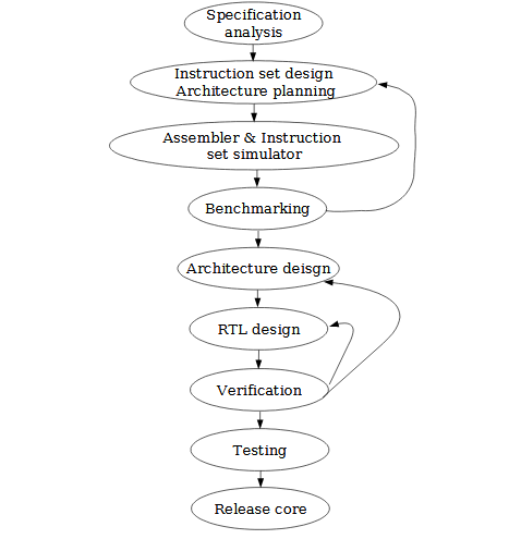
This chapter gives an overview of the design flow of any DSP processor, as well as some certain explanations especially for the designed one. The schematic of the design flow is shown in figure 2.1:
ARCHITECTURE DESIGN
Preview:
A DSP processor can be divided into its processor core and its peripherals. In this job we have concentrated on the processor core design. The core might be divided later into the data path, the control path, the memory, the buses, and the flags.
Research for Media Applications:
According to the design specification we have designed a multimedia DSP processor (MDSP). This is a DSP processor that has special architecture and hardware features to accelerate the media applications. The data have a fixed-point representation. The general structure of the processor is a Harvard’s one, with different memories for programs and for data.
Data Path Organization:
The data path of the designed MDSP consists of two serial data paths and four parallel data paths. The Register file and the memory structure are also described in this sub-chapter.
Control Path:
This sub-chapter gives the overall description of the control path for this processor. In this work we did not concentrate on the detailed design of the control path but have proposed the core’s solutions and root designing features.
The main task of the Control Path is to provide the program flow control. It supplies the correct instruction to execute, decodes instructions into control signals and it manages asynchronous job. It also should supply the correct order of instruction execution by the program counter(PC).
Data Memory:
According to the design specification all memories should be single port SRAM only. This gives the advantage of porting design to different silicon processes. The size of the data memory addressing space should be large enough for covering all functional purposes. Four 16-bit different data accesses are supported in parallel. We have divided the memory bank into four memories (M0, M1, M2, M3).
Flags:
This DSP processor uses a set of four flags that are updated after most of the operations. The flags describe the internal computation status of the processor. They are checked before using the conditional execution instructions.
ADDRESSING DESIGN
Preview:
The task of the address generation unit, AGU, is to generate the correct 16-bit addresses each clock cycle. The AGU is designed so it can access up to four memories at the same clock cycle.
The memories can be accessed with an individual offset between each of them. The data can be addressed with column and row offsets for a very flexible addressing. The AGU also supports Modulo addressing and BRA, bit reversed addressing, as well as most other basic addressing. Exactly what is supported and not is described in this chapter.
Hardware Model:
Two different addresses can be calculated at the same time from two identical address calculation logics inside the AGU. There is a top address register, the TAR, and a bottom address register, the BAR, that supports modulo addressing for each address calculation logic. There is also support for bit reversed addressing, BRA. The BRA supports masking of MSB`s. How many MSB`s that should be masked is checked in the MASK register.
Addressing Model:
There is a set of eight 16-bit address pointer registers, APR0ñAPR7. The memory space in the memory bank is divided into four memories with 64KWords each. We need to address only one 16-bit address pointer to access a word in each memory inside the memory bank. The address can be added with an optional offset.
Addressing Modes:
According to the strategy of addressing, it’s possible to organize a totally flexible offset with a length of up to 16-bits. There are two addressing mode types, the standard and the extended. The standard addressing modes are chosen in the instruction word and the extended are pre-configured in the status register, STATUS.
INSTRUCTION SET DESIGN
Preview:
The instruction set is the interface between hardware and software. The performance of the DSP is heavily dependent on the instruction set. An instruction set must be simple and as orthogonal as possible. If it can be highly orthogonal, then the instruction set is efficient.
The task was to design a set of very few instruction words with instead as many specifiers as possible. The instruction set for this DSP uses eight 32-bit instruction words.
However, we have only used six of them in our design and therefor two of them are reserved for future use. The six instruction words that are used are MOVE, ALU, MAC, DMAC, SIMD and P_FLOW.
ASSEMBLER DESIGN
Preview:
When the structure of the instruction set is defined it’s time for its implementation and verification. It is a very important part of the processor design flow because it shows if the specification requirements are fulfilled or not. The task is in the translation of the input code (assembly code) to the hexadecimal machine code suitable for this processor. For some reasons this process could be named a compiler design.
This chapter is aimed not only on the detailed description of this compiler but also on the tools that have been used during implementation. According to the design specification we have followed the IEEE STD 649-1985 standard to design the assembly code format.
Tools Description:
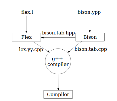
To design the language translator of assembly code to hexadecimal code we have chosen the LEX & YACC tools. The language translator is a program which translates programs that are written in a source language into an equivalent program in an objective language. In our case the source language is the designed assembly code, the object language is the machine code of an actual processor.
Assembler Design Flow:
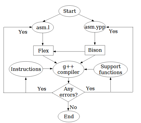
For clear understanding of the Assembler design process take a look at the flow chart diagram shown in figure 6.2. According to the compiler design strategy the parser and the scanner source codes have been generated. A number of auxiliary files are also existed. There are the headers and functions description libraries for the instructions and for the auxiliary functions to perform computations, input/output, debugging.
INSTRUCTION SET SIMULATOR
Preview:
The simulator model is an instruction set simulator, ISS, and is implemented in C++. This programming language was chosen because it’s widely taught and understood. It’s easy to work with and good results can be achieved pretty fast.
If any questions occurs, it’s always easy to find the answers in books and on Internet because C++ is so widely spread and used that there are always somebody else before you that have had the same problems. However, there might be better to use another programming language that has better support for binary programming because this is C++ biggest flaw.
The Start Procedure:
When the ISS starts it will provide the user with three options. The first is to load a file to the program memory, the second is to execute the instructions in the program memory and the third is to quit the simulator program. The start procedure is shown in figure 7.1.
BENCHMARKING
Preview:
Benchmarking is used for revealing strength and weakness of the processors in certain applications. And now, when the instruction set simulator is ready to use, we can check our processor architecture and the instruction set for reaching the specification requirements. The only way of checking is to write some special programs (assembly code) for this processor. As a result of passing this program through the ISS, the number of expended clock cycles are counted.
CONCLUSIONS
From the beginning of this final year project we aimed for designing a high performance DSP with accelerated media functions. We soon realized that this was impossible with the limited time that was offered. We decided to focus on the SIMD part of the design and all our results are based on this.
In fact, we have designed the processor’s core according to a given specification. We have researched the possibility’s for hardware accelerating of media DSP applications. The complete instruction set for the designed processor is presented in this work (except interrupts handling).
The instruction set simulator was designed only for SIMD parallel computational paths of the processor. We have stopped at the benchmarking design step due to lack of time and have not completely verified our architecture and instruction set. That is why we can’t release the performance results and can only expect them according to our research efforts.
The designed processor should show good performance for 8/16-bit convolution based algorithms. The motion estimation and compensation (MPEG) applications should also be solved very well because of the architectural improvements made especially for them. The designed addressing models gives the opportunity to process the multidimensional media algorithms with a high-level of flexibility of the data accesses.
The high level of orthogonality of the instruction set and the architecture gives the designers the possibility of using all available (6!!!) data paths simultaneously. In this way, six different results are calculated at the same time, four loop results to the memories, and two auxiliary register operations.
The SIMD parallel data paths can process 8-bit media data with a great performance for non high-quality color applications, up to five significant bits per pixel. To process data with high-quality colors, programmersshould use the DMAC mode.
In addition, the sophisticated ALU unit offers the possibility to speed up the execution of logic, arithmetic, and shift operations. The designed instruction set is quite flexible for future improvements and changes media algorithms with a high-level of flexibility of the data accesses.
FUTURE WORK AND IMPROVEMENTS
All incomplete issues and activities for this processor should be finished in order to release the core. Completing the architecture and implementing it in RTL code with a following verification. In the SIMD part, the memory accessing could be changed for a more flexible way to address data.
In our design, when working with 8-bit data, we store two operands in each memory line. However this is not good for some applications where we have to multiply the data with coefficients as in FFT, FIR for example. It would be better if we could access two 8-bit operands from different memories instead.
In this case we could use two memories that contains the data and the other two can contain the coefficients. If this is done and we use modulo addressing on the coefficient memories, then the performance of coefficient based applications can be greatly improved.
In our research we did not pay attention on the interrupts handling. Interrupts of course are necessary for proper processor’s exploitation. The direct memory access (DMA) unit could significantly improve the total processor performance due to data memory accesses are always the bottleneck.
Source: Linkoping University
Authors: Vladimir Gnatyuk | Christian Runesson


