ABSTRACT
Three-dimensional information of the burden surface in high temperature and excessive dust industrial conditions has been previously hard to obtain. This paper presents a novel microstrip-fed dielectric-filled waveguide antenna element which is resistant to dust and high temperatures. A novel microstrip-to-dielectric-loaded waveguide transition was developed.
A cylinder and cuboid composite structure was employed at the terminal of the antenna element, which improved the return loss performance and reduced the size. The proposed antenna element was easily integrated into a T-shape multiple-input multiple-output (MIMO) imaging radar system and tested in both the laboratory environment and real blast furnace environment. The measurement results show that the proposed antenna element works very well in industrial 3D imaging radar.
WORKING FREQUENCY SELECTION
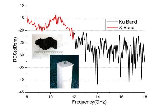
Figure 1. The radar cross-section (RCS) test result of the coke sample
We measured the RCS of a typically sized coke at 8–18 GHz in compact antenna test range (CATR) in Beihang University (Beijing, China). The dimensions of the coke being tested were about 120 mm × 80 mm × 70 mm. The measurement result is shown in Figure 1. From the result, it was determined that the porous carbon has an absorption effect on microwaves, and the reflection decreases with increasing frequency.
ANTENNA ELEMENT DESIGN CONCEPT
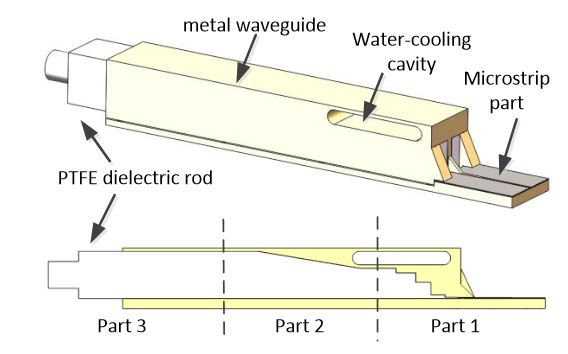
Figure 2. Structure of the proposed antenna element
The geometry of the proposed antenna element is shown in Figure 2. It is a microstrip-fed dielectric-filled waveguide antenna element. The microstrip direct feed circuit saves microwave connectors and precisely controls amplitude and phase at a low cost. The Polytetrafluoroethylene (PTFE) dielectric rod within the metal waveguide reduces the cutoff frequency and isolates the feed circuit from the outside dust and high temperature environment which performs sealing function.
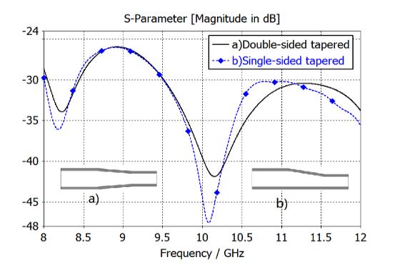
Figure 5. Return loss of different type transformers
Square cross-section of the waveguide was applied in order to achieve substantially equal E-plane and H-plane radiation patterns. A transformer was required to suppress reflection between the rectangular waveguide and square waveguide. Two different tapered waveguide transformers were used for the rectangle-waveguide-to-square-waveguide. The simulation results are shown in Figure 5.
PROTOTYPE MEASUREMENT
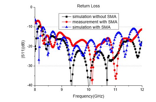
Figure 7. The reflection characteristics of the proposed antenna element
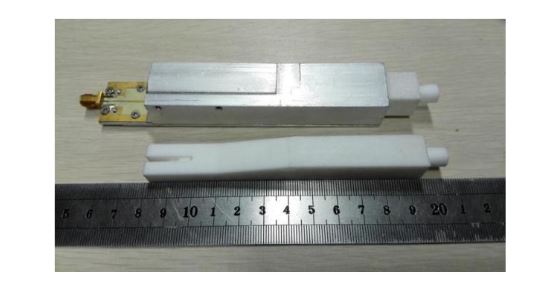
Figure 8. Photograph of a prototype of the proposed antenna element
The whole antenna element was simulated and the reflection characteristics are shown in Figure 7. The return loss of the whole antenna is below −20 dB from 9.2 GHz to 11.2 GHz. A prototype of the antenna based on the concept was fabricated as shown in Figure 8. The antenna element has been measured in CATR of Electromagnetic Engineering Laboratory, Beihang University.
ARRAY ARRANGEMENT METHOD
The four arrays can obtain the same equivalent virtual array. The square type I array has the complex feed network and the cross type array has the two arrays cross at the central point. The square type II array has the smallest actual array size and has great potential to be used in our future systems.
The T type array has the simplest feed network and is capable of using planar array feed technology. In addition, the vertical distance between transmitting array and receiving array in T type array is does not need to be strictly limited as in the other three arrays, so its advantage is that the distance can be increased appropriately to reduce the mutual coupling between the transmitting array and the receiving array.
MIMO IMAGING RADAR FABRICATION AND TESTING
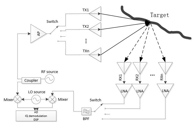
Figure 11. The system block diagram of the imaging radar
The system block diagram of the imaging radar is shown in Figure 11. The system contains 16 transmit antennas and 16 receive antennas, two 1:16 switch matrices, and one microwave receiver. The transmit antennas and receive antennas form switched arrays which are switched through microwave switches. The wideband microwave signal transmitted by one transmit antenna is reflected by the target, and the echo signal is received by the 16 receive antennas in sequence.
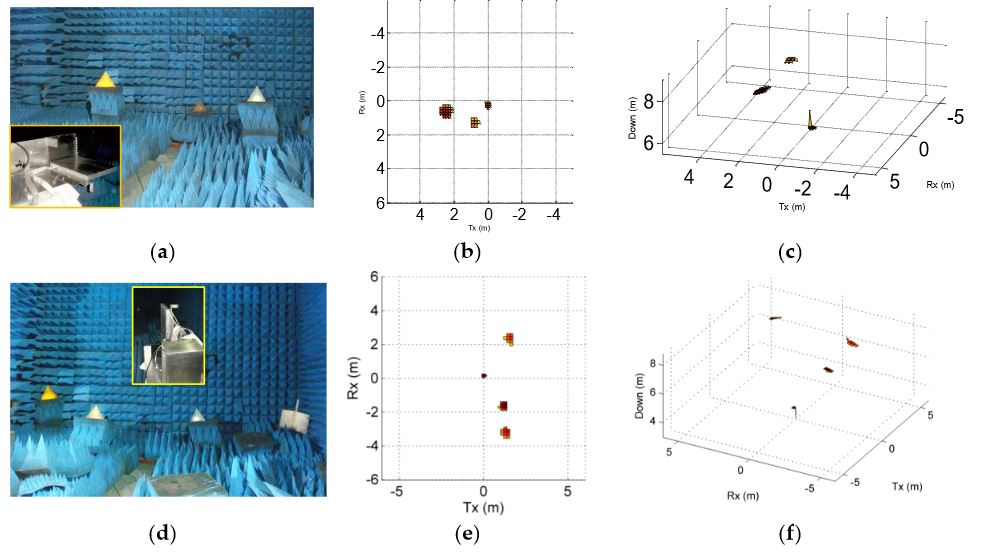
Figure 13. Test scenarios and 3D imaging results (a) Tx array placed in horizontal direction with three reflectors
Arrangement of test scenarios and test results are shown in Figure 13. It can be seen that the radar can image in wide angles in both directions, and the imaging results coincide with the target arrangement position. The result shows that the T-shape MIMO radar built with the proposed antenna elements can be used for 3D measurement and high accuracy images are achieved.
CONCLUSIONS
A novel dielectric-filled waveguide antenna element for 3D burden surface imaging industrial radar is proposed in this paper. The relationship between frequency and the reflection characteristics of the main material has been studied and the working frequency of the antenna has been chosen. The metal waveguide shell with water-cooling cavity and the filled dielectric can separate the feed circuits from high temperatures and dust.
An air gap is used to improve the impedance matching for microstrip-to-ridged-waveguide transition. A novel dielectric radiation segment—including a square column and a cylinder dielectric rod—extending out of the waveguide was developed. The geometry provides better return loss performance and higher reliability compared to traditional tapering dielectric rod antennas.
According to the simulated result, a prototype of the antenna element working at X-band was fabricated and tested. Good accordance is obtained between simulated and measured results. A prototype of a T-shape 3D imaging MIMO radar was designed and assembled. The MIMO radar was tested both in the laboratory environment and real blast furnace environment. The measurement results show that the radar can obtain relatively accurate 3D burden surface information in harsh environments.
Source: Beihang University
Authors: Ding Xu | Zhiping Li | Xianzhong Chen | Zhengpeng Wang | Jianhua Wu
>> Project Report on Microstrip Patch Antenna for Final Year Students