ABSTRACT
In this paper, a silicon-based radio frequency micro-electromechanical systems (RF MEMS) pattern reconfigurable antenna for a Ka-band application was designed, analyzed, fabricated, and measured. The proposed antenna can steer the beam among three radiating patterns (with main lobe directions of −20◦, 0◦, and +20◦ approximately) at 35 GHz by switching RF MEMS operating modes.
The antenna has a low profile with a small size of 3.7 mm × 4.4 mm × 0.4 mm, and consists of one driven patch, four parasitic patches, two assistant patches, and two RF MEMS switches. The active element pattern method integrated with signal flow diagram was employed to analyze the performances of the proposed antenna. Comparing the measured results with analytical and simulated ones, good agreements are obtained.
DESIGN OF THE PATTERN RECONFIGURABLE ANTENNA
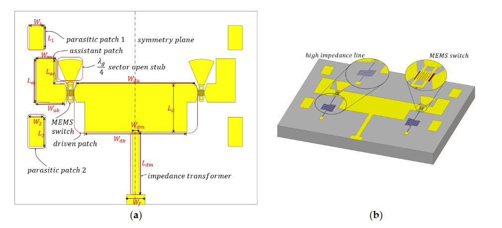
Figure 1. Proposed pattern reconfigurable antenna. (a) The configuration of proposed antenna. (b) The 3D view of the proposed antenna
A pattern reconfigurable is designed and its structure is illustrated in Figure 1, the close-ups shown in Figure 1b are the RF MEMS switch and its DC actuating circuit. The geometry configurations of Figure 1a are shown in Table1. The antenna consists of one rectangle driven patch radiator, four rectangle parasitic patches, two assistant patches, and two RF MEMS switches.
THEORY ANALYSIS OF PATTERN RECONFIGURATIONS
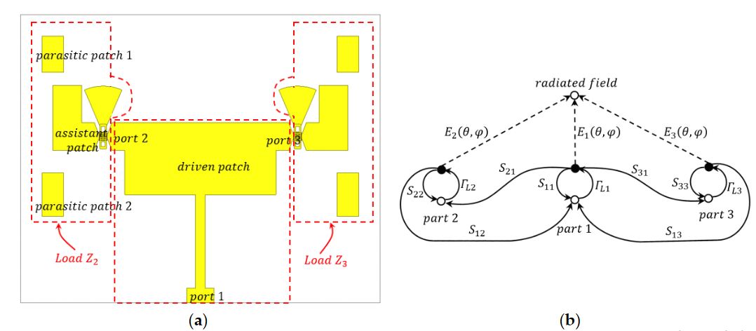
Figure 3. Divided parts of the antenna and its signal flow diagram. (a) Divided parts of the antenna. (b) Equivalent signal flow diagram of the proposed pattern reconfigurable antenna
An antenna array can be fully described by its scattering parameters and the active element pattern of each radiating element. The proposed pattern reconfigurable antenna in this paper can be viewed as the degenerated antenna array shown in Figure 3a. (The whole structure of the reconfigurable antenna can be divided into three parts shown in Figure 3a, i.e., the left part, middle part, and right part.
FABRICATION, MEASUREMENT, AND RESULTS
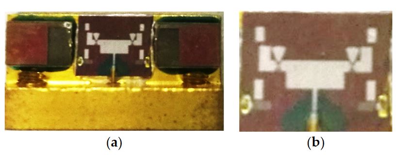
Figure 6. The photograph of the proposed pattern reconfigurable antenna taken by a microscope. (a) The antenna with testing holder. (b) Close-up of the antenna
A 1.5-μm-thick layer of Al, which acts as an anchor, is evaporated. Polyimide as the sacrificial layer was cut down by a chemical mechanical polishing (CMP) process. The beam uses 0.6 μm of SiAl. Finally, the wafer is released in a plasma dryer to avoid the collapse of the membrane. The photographs of the proposed antenna and its close-up are shown in Figure 6.
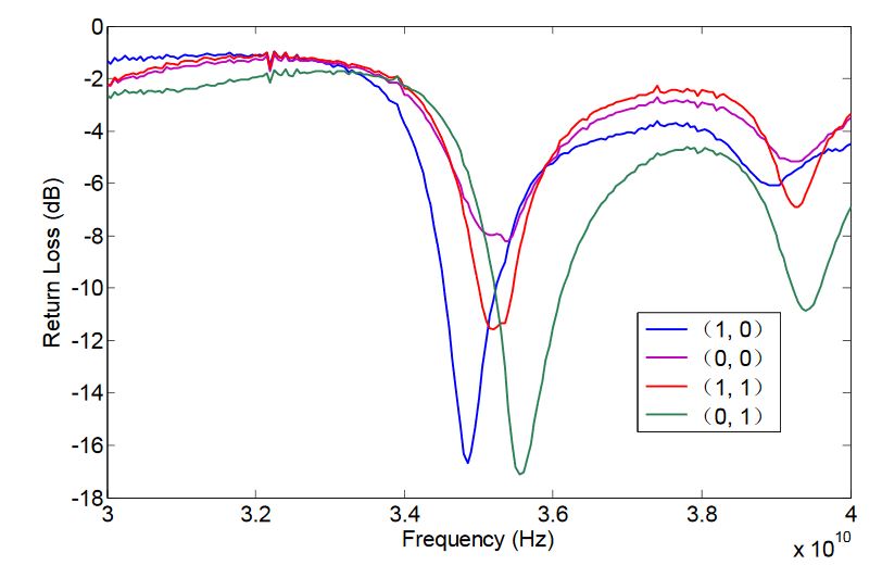
Figure 7. The measured return loss of the proposed pattern reconfigurable antenna in all states of the RF MEMS switches
Input impedance of all operating modes at the desired frequency of 35 GHz is essential. The return loss of the proposed antenna was measured with the network analyzer Agilent PAN N5442A. The antenna was fed with a 50 Ω microstrip line, and the input impedance of the antenna was transformed by a transformer. The measured return losses of all modes were approximately 10 dB at the desired frequency of 35 GHz, as shown in Figure 7.
CONCLUSIONS
This paper proposes a pattern reconfigurable antenna by employing two RF MEMS switches. By changing the two RF MEMS operating modes, the proposed antenna can switch among three kinds of reconfigurable patterns, namely middle (approximately 0◦), left (approximately −20◦), and right (approximately 20◦). The proposed pattern reconfigurable antenna was analyzed using an active element pattern method and a signal flow diagram.
Comparing the measured results with the calculated and simulated results, good agreement was obtained. The proposed pattern reconfigurable antenna can be applied to a 5th-generation (5G) mobile communication and satellite communication system because of its excellent performance.
Source: Beijing University
Authors: Ke Han | Zhongliang Deng | Xubing Guo
>> 60+ Antenna Communication Projects for Engineering Students
>> Antenna Based Projects List for Engineering Students
>> Antenna Design Projects for Engineering Students