ABSTRACT
This paper describes the design of a high-efficiency energy harvesting circuit with an integrated antenna. The circuit is composed of series resonance and boost rectifier circuits for converting radio frequency power into boosted direct current (DC) voltage. The measured output DC voltage is 5.67 V for an input of 100 mV at 900 MHz. Antenna input impedance matching is optimized for greater efficiency and miniaturization. The measured efficiency of this antenna-integrated energy harvester is 60% for −4.85 dBm input power and a load resistance equal to 20 k Ω at 905 MHz.
CIRCUIT DESIGN
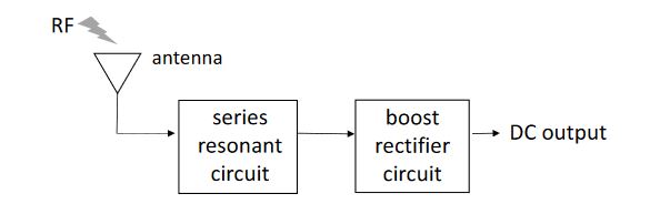
Figure 1. Block diagram of the energy harvesting circuit. RF: radio frequency
Figure 1 shows a block diagram of the proposed energy harvesting circuit with an antenna. The antenna with optimized input impedance, the series resonance circuit, and the boost rectifier circuits are all connected to each other. The weak input RF signal is amplified by the impedance matching circuit and series resonance circuit to obtain the DC output voltage.
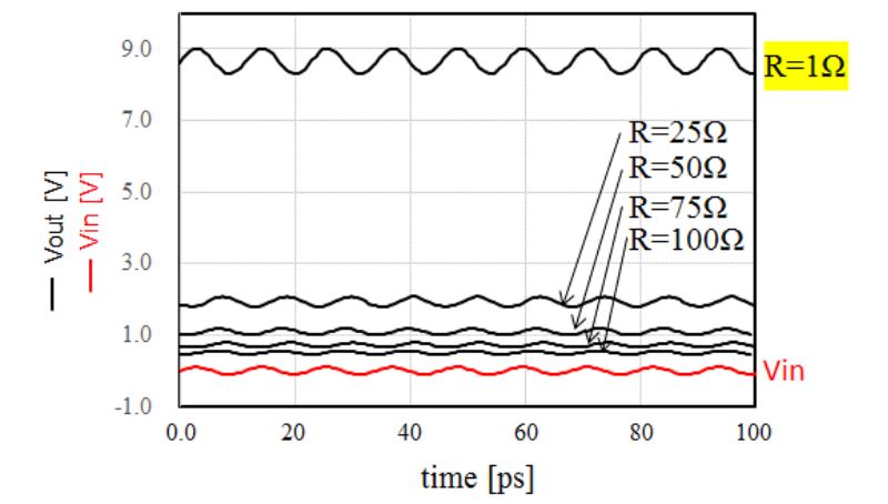
Figure 5. Transient simulation of the output voltage with different antenna impedances
Considering Equation (2), the Q value is increased when R decreases. Thus, the input voltage is amplified and efficiency is also increased by changing the value of R. Figure 5 shows the time-domain simulation results in the steady-state of the DC voltage of the proposed circuit shown in Figure 2. As shown in Figure 5, when the antenna impedance R decreases, the DC output voltage increases. For the simulation, when R is less than 1 Ω, it is regarded as short.
CIRCUIT-MEASURING METHOD
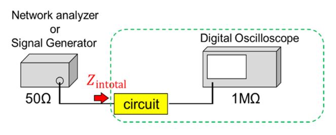
Figure 6. Simplified diagram of measurement
The reflection effect calculation method is shown as follows. To calculate this effect, it is necessary to measure the input impedance. Thus, the input impedance of the measurement system is measured by using a network analyzer. Here, the measurement system of the proposed circuit, coaxial cable, and digital oscilloscope is indicated by a dotted circle in Figure 6.
CIRCUIT MEASUREMENT
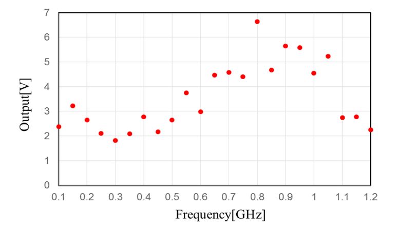
Figure 8. Measurement output voltage versus input RF signal
Figure 8 shows the measurement results of the output DC voltage at a load resistance equal to 1 M Ω with different input frequencies. As shown in Figure 8, the DC output voltage is boosted for 100 mV of input. The output voltage is highly boosted for 800 MHz to 1.05 GHz and the central frequency of the higher-boosted voltage frequency is around 900 MHz. Therefore, the DC output voltage of this circuit is 5.67 V for a 900-MHz, 100-mV alternating current (AC) input.
POWER-CONVERSION EFFICIENCY MEASUREMENT
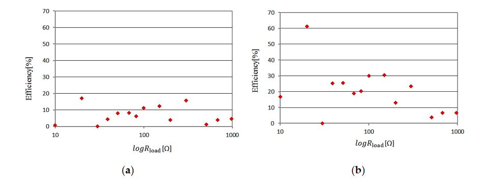
Figure 9. Measurement output voltage versus input RF signal. (a) Input voltage is 50 mV (b) input voltage 100 mV
Figure 9 shows the measurement results. Two cases of the input power into the measurement system (50 mV and 100 mV) are shown as examples. When the value of the load resistance is 20 kΩ, the maximum efficiency is 17.2 % and 61.2 % for the 50 and 100 mV inputs, respectively. Therefore, the optimal value of the load resistance is 2.
ANTENNA DESIGN
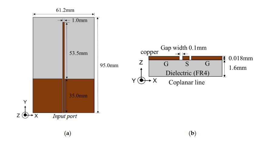
Figure 10. Layout of the proposed antenna. (a) layout, (b) cross sectional view
The antenna requirements are an input impedance of 1 Ω and a unidirectional radiation. Figure 10 shows the layout of the proposed antenna. This antenna is a quarter wavelength monopole antenna with a CPW transmission feed line and a one-sided metal layer. Considering the current flow of the monopole antenna, it is open-edged and short in the port. Moreover, the radiation pattern of the monopole antenna is unidirectional.
ANTENNA IMPEDANCE MEASURING METHOD
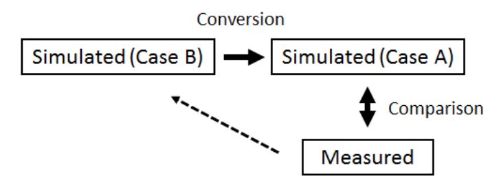
Figure 12. Block diagram of the measuring method of the proposed antenna
Figure 12 shows the block diagram of the measuring method. The calculation results of Case B are converted to Case A, and then compared to the measurement results. If they correspond to each other, the characteristics of the fabricated antenna and Case B are equal. The conversion of Case B to Case A means calculating the characteristics for changing measurement conditions only. First, the characteristics of S11 and the radiation pattern are calculated under Case A and B. The simulation results are then compared to the measured results.
ANTENNA MEASUREMENT
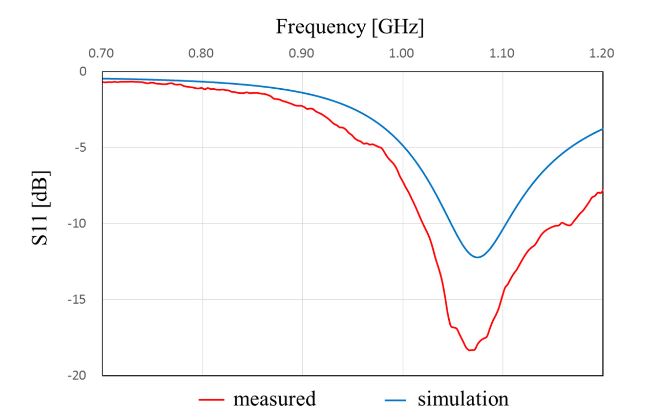
Figure 13. Frequency characteristics of S11 of the proposed antenna in Case A
Figure 13 shows the measured and simulated Case A characteristics of S11. The measured peak frequency corresponds to the simulated results. The value of S11 is slightly shifted, and the impedance approaches 50 Ω because of the soldering effect of the connector.
INTEGRATION OF THE ANTENNA AND THE CIRCUIT
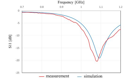
Figure 17. Frequency characteristics of S11 of the antenna with an impedance matching circuit
Figure 17 shows the simulation result of the S11. From this result, S11 is less than −10 dB. Namely, the transmission rate is more than 90% from 875 MHz to 915 MHz. Therefore, impedance matching between the antenna and the circuit is confirmed at 905 MHz.
MEASUREMENT OF THE ANTENNA WITH IMPEDANCE MATCHING CIRCUIT
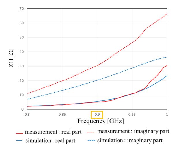
Figure 19. Frequency characteristics of Z11 of the proposed antenna with impedance matching circuit calculated from s-parameters
Figure 19 shows the measured and simulated Case C impedance Z11 calculated from S11. From this result, the real part of the measured result is approximately equal to that of the simulated Case C at 900 MHz. On the other hand, the measured imaginary part is slightly higher than that of the simulated result because of the error from the parasitic elements of soldering.
OPERATION CONFIRMATION OF THE CIRCUIT INTEGRATED WITH AN IMPEDANCE MATCHING ANTENNA
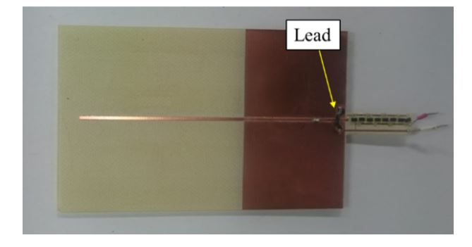
Figure 20. Photograph of the fabricated antenna with the impedance matching antenna
Figure 20 shows a photograph of the fabricated antenna and circuit on the same substrate. A ground line of the circuit is connected to one ground of the antenna. Thus, grounds are connected by using a lead line.
CONCLUSIONS
In this study, a high-efficiency energy harvester was developed. For the boost rectifier circuit, the DC output voltage is 5.67 V for input voltage of 100 mV AC and 900 MHz. A low-input impedance antenna was successfully developed. In addition, we formulated the antenna measurement method, integrated the circuit, and impedance-matched the antenna. This final efficiency is 60% for a load resistance equal to 20 kΩ when the input power is −4.85 dBm.
Source: Kyushu University
Authors: Yuharu Shinki | Kyohei Shibata | Mohamed Mansour | Haruichi Kanaya