ABSTRACT
Cold-cathode electron field emission is a technology emerging as an appealing alternative to high power thermionic emitters and gas plasma contactors that use a consumable (Xe gas, typically) for space electrodynamic tether systems and other space electric propulsion systems requiring low-power neutralizers.
Example cold-cathode electron field emission technologies include Spindt-type cathodes and gated carbon nanotubes, both of which emit electrons through quantum mechanical tunneling of electrons, instigated by a high electric field applied at the emitter surface. Research at the University of Michigan indicates that nano structured Boron Nitride (BN) is an attractive material for cold-cathode electron emission due to its low work function, structural robustness, chemical inertness (Spindt-type cathodes with Mo tips are known to degrade in an oxygen environment), and favorable emission characteristics.
To facilitate the acceleration of electrons away from the emission surface and toward the plasma anode (beyond the space charge limit), a MEMS-based gated structure has been developed in order to provide the high surface electric fields required for electron emission at the BN surface. This paper will describe the integrated device development for a gated-BN emitter to be used in the student-designed Field Emission Get-Away-Special Investigation (FEGI) project-a test platform for low-earth demonstration of various cold-cathode electron field emitter designs.
THIN FILM EMISSION SURFACES
A gated structure has been developed to enhance electric fields over a thin film emission surface. Minor modifications to the existing gate can allow for integration with almost any planar emission surface with surface roughness less than 100Å. The initial gate design was developed around the properties of BN emitters, because research at the University of Michigan shows thin film Boron Nitride (BN) to be a favorable emission surface.
GATE DESIGN AND FABRICATION
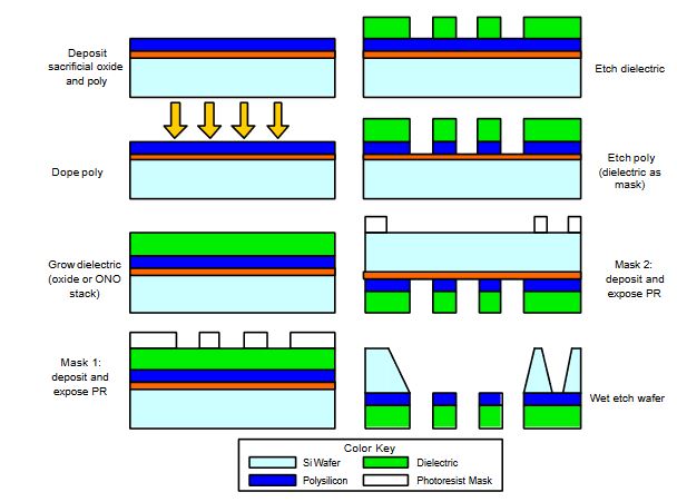
Figure 2. Gate fabrication sequence
The gate structure is fabricated using a two-mask process, as shown in Figure 2. The gate is released in a dissolved wafer process (DWP), and is therefore created upside-down in fabrication. The individual fabrication steps are well characterized from semiconductor fabrication; however there are a number of fabrication challenges due to small feature sizes and delicate structures on the devices themselves.
FIELD EMISSION GET-AWAY-SPECIAL INVESTIGATION (FEGI)
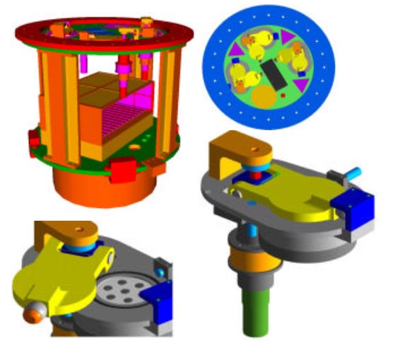
Figure 4. FEGI Experiment. BN gated emitters will be placed inside vacuum enclosures
The FEGI experiment is being developed at the University of Michigan under the student-run Student Space Systems Fabrication Lab (S3 FL). The experiment is designed to fly on the Space Shuttle as a Get Away Special payload, and will serve as a testbed for cold-cathode field emitters used in low earth orbit. One of the many field emitters flown on FEGI will be a gated Bor on Nitride field emitter. The FEGI experiment requires flown field emitters to conform to the form factor of a standard TO-5 transistor header.
FUTURE DEVELOPMENT
The next stage of development is the integration of the gate with a BN emitting surface. Emission tests will be performed in a high vacuum chamber to see how the gate improves emission efficiency. Further iterations of the gate design may be necessary to further characterize fabrication parameters to produce gates with better dielectric thicknesses, hole diameters, and hole densities for emission area.
CONCLUSION
A new gated structure has been developed to assist and improve cold cathode electron emission from a variety of thin film surfaces. With this gated structure, integrated devices of Boron Nitride, carbon nanotube, and other thin emitting films will be made with higher system efficiency and lower turn-on voltage than previous designs. Initial testing will be performed in the laboratory with BN and compared with previous results. The upcoming FEGI Shuttle mission at the University of Michigan will provide a test bed for this new structure mounted over BN (along with other cold cathode emitters).
Source: University of Michigan
Authors: H. Goldberg | P. Encarnacion | D. Morris | B. Gilchrist | R. Clarke