ABSTRACT
The Elliptic Curve Digital Signature Algorithm (ECDSA) is the analog to the Digital Signature Algorithm (DSA). Based on the elliptic curve, which uses a small key compared to the others public-key algorithms, ECDSA is the most suitable scheme for environments where processor power and storage are limited. This paper focuses on the hardware implementation of the ECDSA over elliptic curves with the 163-bit key length recommended by the NIST (National Institute of Standards and Technology). It offers two services: signature generation and signature verification.
The proposed processor integrates an ECC IP, a Secure Hash Standard 2 IP (SHA-2 Ip) and Random Number Generator IP (RNG IP). Thus, all IPs will be optimized, and different types of RNG will be implemented in order to choose the most appropriate one. A co-simulation was done to verify the ECDSA processor using MATLAB Software. All modules were implemented on a Xilinx Virtex 5 ML 50 FPGA platform; they require respectively 9670 slices, 2530 slices and 18,504 slices.
FPGA implementations represent generally the firststep for obtaining faster ASIC implementations. Further, the proposed design was also implemented on an ASIC CMOS 45-nm technology; it requires a 0.257 mm2 area cell achieving a maximum frequency of 532 MHz and consumes 63.444 (mW). Furthermore, in this paper, we analyze the security of our proposed ECDSA processor against the no correctness check for input points and restart attacks.
RELATED WORKS
This section focuses on the previous state-of-the-art ECDSA implementations. In the literature, only a small number of full ECDSA implementations has been reported. To ensure the authentication and verification scheme for the IEEE Wireless Access in Vehicular communication (WAVE), which is based on Vehicular Adhoc Networks (VANETs), the authors launch in the vehicular message authentication and the prioritized verification for periodic safety messages. They developed the ECDSA mechanism incorporating an Identity-based (ID-based) signature. However, the authors in their work did not mention this and studied the IPs used in the signature process.
ECDSA PROCESSOR METHODOLOGY AND FLOW DESIGN
Figure 1 resumes the design flow of the digital signature proposed in this paper. Using the mentioned design flow, to develop and to design a secure digital signature processor.
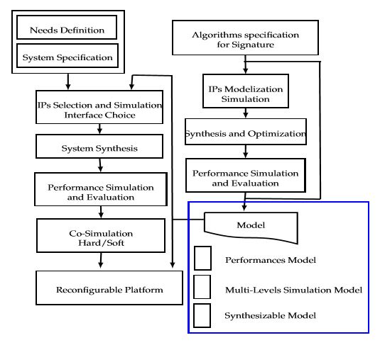
Figure 1. The proposed methodology and flow design of the Elliptic Curve Digital Signature Algorithm (ECDSA)
PROPOSED HARDWARE ARCHITECTURE FOR ECDSA IPS
Simulation and Synthesis Results of Ecc Ip
The implementation of is recent, it was done in 2015 using the Virtex5 platform, our proposed ECC architecture presents better results in all parameters. In fact, the area and time are decreased by 6.68% and 49.4% respectively. The last two columns in the table show the algorithmic throughput and efficiency. In order to compare our design to those of the other works we draw the Figure 4 containing both throughput and efficiency values.
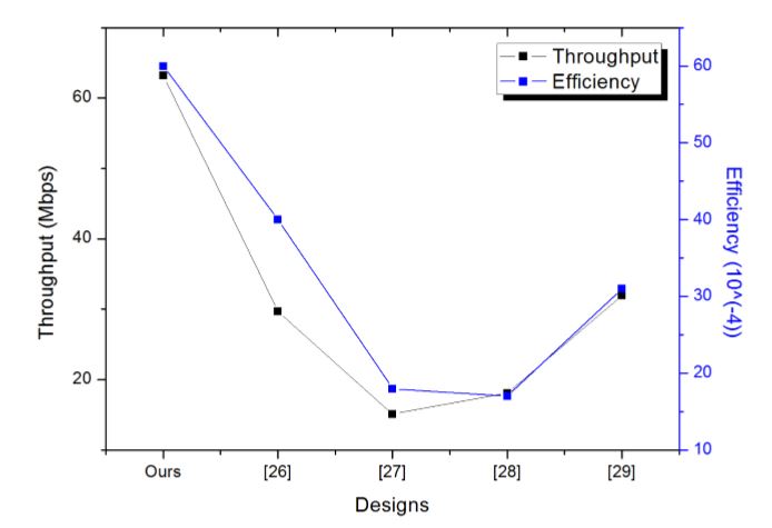
Figure 4. Throughput and efficiency comparison
The two registers (LFSR and NLFSR) of the grain are synchronized such that a bit is generated each clock cycle. The grain offers the possibility to increase the speed thanks to the implementation of polynomial functions (f(x) and g(x)) and the filter function (h(x)) several times. Hence, to simplify this implementation, the last 15 bits of the two shift registers (si and bi,65≤i≤79) were used neither in f(x) and g(x) functions, nor in the filter function input. Thus, this can multiply the speed by 16 and reduce the initialization phase required time (160/16cycles) and the keygeneration (80/16cycles). Figure 7 shows a sample implementation: in a doubling, two bits are generated at each clock cycle.
Figure 7. Doubling-speed Grain Scheme
ECDSA ARCHITECTURE FOR LOW-AREA LOW-POWER COMPUTING
Proposed Ecdsa Processor Design
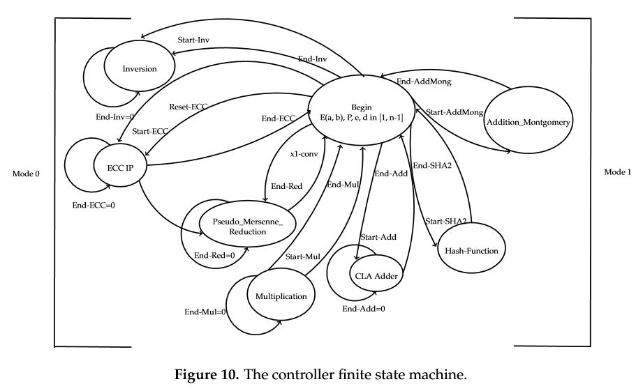
Figure 10. The controller finite state machine
Thus, an efficient hardware implementation needs the synchronization of the different components as shown in the Figure 10. The controller uses two modes: Mode 0 for the key and the signature generation and Mode 1 for the signature verification. All used blocks need two signals: “Start” to begin the computation and “End” to end the computation.
IMPLEMENTATION RESULTS OF ECDSA AND PERFORMANCE ANALYSES
In order to have a relevant performance comparison between our synthesis results and those of related works, we will add another parameter which is the Area Time Product (ATP). Figure 11 gives different ATP of the mentioned state-of-the-art FPGA implementations.
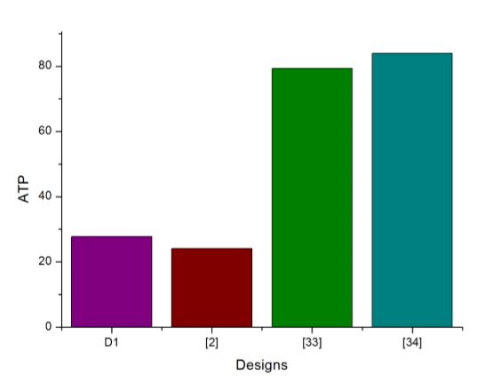
Figure 11. FPGA Implementation ATP
SECURITY ANALYSES OF ECDSA PROCESSOR
The Elliptic Curve Discrete Logarithm Problem (ECDLP) is a special case of the discrete logarithm problem. It consists of finding an integer d, if it exists, such that Q = dG, given points G, Q ∈ E(Fq). Many attacks against ECDLP exist such as the exhaustive search, the Pohlig-Hellman, and the Baby-Step Giant-Step algorithms. One of these attacks is the Pollard’s Rho algorithm, which has a running time of√nπ/2 where n is the order of point G. However, this algorithm can be parallelized and run on r different processors, so that the new running time is√nπ/2r.
CONCLUSIONS AND FUTURE WORKS
In this paper, an ECDSA signature scheme was implemented. All integrated IPs (ECC, SHA-2, and the grain) were optimized in order to lead to a trade-off between area and execution time. Thus, the implementation results, in both Virtex-5 and ASIC, are competitive with those of the state-of-the-art. The signature and the verification processor used 18, 504 slices in Virtex-5 achieving a frequency of 107.4 in1.5 µs.
Being implemented on an ASICCMOS45 nm technology, the design requires 0.257mm2 area cell achieving a maximum frequency of 532 MHz and consumes 63.444 (mW). The proposed ECDSA implementation is suitable for applications that need: low-bandwidth communication, low-storage and low-computation environments such as embedded systems. As we said earlier, the design overhead costs should be reduced to be suitable for applications which require low area resources. As a future work, ECC-IP can be again optimized by introducing the procedure of Secure Hardware Activation System (SEHAS) and the Physically Unclonable Functions (PUF).
Source: University of Monastir
Authors: Anissa Sghaier | Medien Zeghid | Chiraz Massoud | Mohsen Machout
>> More Analog Communication Projects using Matlab for Engineering Students
>> More Matlab Engineering Projects based on Wireless Communication for Students
>> For More Matlab Projects on Embedded Systems for Final Year Students
>> More Wireless Projects based on Fpga for Final Year Students