ABSTRACT
This paper investigates the feasibility of a backend design for real-time, multiple-channel processing digital phased array system, particularly for high-performance embedded computing platforms constructed of general purpose digital signal processors. First, we obtained the lab-scale backend performance benchmark from simulating beamforming, pulse compression, and Doppler filtering based on a Micro Telecom Computing Architecture (MTCA) chassis using the Serial RapidIO protocol in backplane communication.
Next, a field-scale demonstrator of a multifunctional phased array radar is emulated by using the similar configuration. Interestingly, the performance of a barebones design is compared to that of emerging tools that systematically take advantage of parallelism and multicore capabilities, including the Open Computing Language.
BACKEND SYSTEM ARCHITECTURE
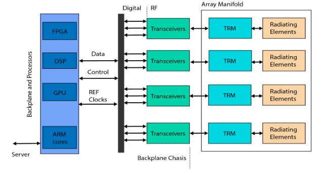
Figure 1. Top-level system digital array system concept
Moreover, the connection topology among each processing and I/O module should be flexible and capable of switching a large amount of data from other boards. Figure 1 shows a top-level system description of a general large-scale array radar system. In receiving arrays, once data are collected from the array manifold, each transmit and receive module (TRM) downconverts the incoming I/Q streams in parallel.
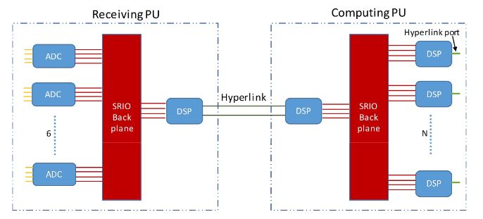
Figure 4. Simple example of a processing unit (PU)-based architecture
We currently operate an example of a receiving digital array at the University of Oklahoma (Figure 4) with two types of PUs—namely, a receiving (i.e., data acquisition) PU and a computing PU. In the receiving PU, six field-programmable RF transceiver modules (e.g., VadaTech AMC518 + FMC214) sample the analog returns from TRM and send the digitalized data to a DSP module by way of an SRIO backplane.
REAL-TIME IMPLEMENTATION OF A DIGITAL ARRAY RADAR PROCESSING CHAIN
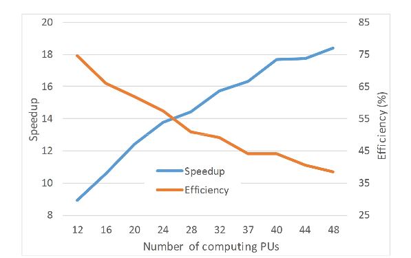
Figure 11. Speedup and efficiency of beamforming implementation
Figure 11 shows the performance of beamforming by using different numbers of PUs as an example, in which Nc = 480 and Nrg = 1024. In this figure, the speedup and efficiency is calculated according to Equations (1) and (2), in which the speedup grows with the number of PUs, but the efficiency is degraded due to the method call overhead.
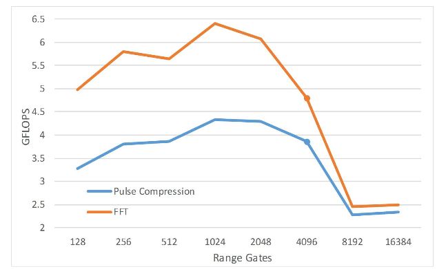
Figure 13. Performance of pulse compression and fast Fourier transform (FFT) vs. different numbers of range gates
The computation throughput of pulse compression and FFT measured on one C66xx core is shown in Figure 13, in which dots represent the maximum number of range gates that the L1D cache can hold. It is evident that the calculation performance would degrade dramatically when the data size is close to or over the cache size, and the performance of pulse compression and FFT correlates to each other.
PERFORMANCE ANALYSIS OF COMPLETE SIGNAL PROCESSING CHAIN
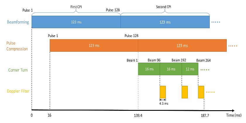
Figure 14. Real-time system timeline for the example backend system
This latency confines the shortest PRI that the backend system allows for real-time processing. Based on the parameters in Table 5, the time scheduling of the radar processing chain is shown in Figure 14. This scheduling is a rigorous and realistic timeline including all of the impacts of SRIO communication and memory access, and has been verified by real-time hardware running tests. The numbers of PU and PE are chosen as an example, which can be changed based on different requirements.
PARALLEL IMPLEMENTATION USING OPEN COMPUTING LANGUAGE (OPENCL)/OPEN MULTI-PROCESSING (OPENMP)
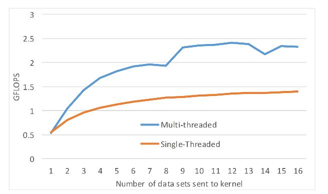
Figure 15. Beamforming kernel performance using Open Computing Language (OpenCL) (8192 range gates)
For beamforming, we design to make the kernel processes an arbitrary number of datasets; in each dataset, it contains the sampled return data from 24 channels. The processing of each set is allocated to its OpenMP thread. Figure 15 shows that as the number of datasets sent to the kernel increases, the time it takes to form a beam from each set decreases.
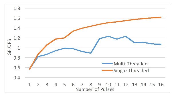
Figure 17. Pulse compression performance using OpenCL (8192 range gates)
In pulse compression, once again the kernel can receive an arbitrary number of pulses. Each beam is processed in its OpenMP thread. However, in this case, multi-threaded execution is not favorable as shown in Figure 17. This difference is due to the highly non-linear memory accesses required by the FFT and IFFT.
SUMMARY
In this study, we present a development model of an efficient and scalable backend system for digital PAR based on Field-Programmable-RF channels, DSP core, and the SRIO backplane. The architecture of the model allows synchronized and data-parallel real-time surveillance for radar signal processing. Moreover, the system is modularized for scalability and flexibility. Each PE in the system has a proper granularity to maintain a good balance between computation load and communication overheads.
Even for the basic radar processing operations studied in this work, tera-scale floating point operations are required in the MPAR-type backend system. For such requirement, using software programmable DSPs that can be attuned to the processing assignment in parallel would be a good solution. The computational aspects of a 7400 GFLOPS throughput phased array backend system have been presented to illustrate the analysis of the basic radar processing tasks and the method of mapping those tasks to an MTCA chassis and DSP hardware.
In our implementation of a PAR backend system, the form-factor can be changed based on requirements of various systems. By changing the number of PUs, the total capacity of the system can be easily scaled. By changing the number of inputs for each PE, we can adjust the throughput performance of a PU. A carefully customized design of different processing stages in the DSP core also helps to achieve the optimal performance regarding latency and efficiency.
When we parallelize a candidate algorithm, there are two steps in the design process. First, the algorithm is decomposed into several small components. Next, each algorithm component is assigned to different processors for parallel execution. In parallel computing, the communication overhead among parallel computing nodes is a key impact on the parallel efficiency of the system. Within each parallel processor, dividing the entire data cube into small subsets to avoid cache miss is also necessary when the size of input data is larger than the cache size of processors.
For data communication links, the SRIO, HyperLink, and EDMA3 handle the data traffic between and/or within each DSP. By using SRIO, the data traffic among DSPs can be switched through the SRIO fabric controlled by an MCH of the MTCA chassis, which is more flexible than PCIe and efficient than Gigabit Ethernet. A novel advantage of our proposed method is utilizing EDMA3 and the ping-pong buffer mechanism, which helps the system to overlap the communication time with computing time and reduce the processing latency.
Source: University of Oklahoma
Authors: Xining Yu | Yan Zhang | Ankit Patel | Allen Zahrai | Mark Weber