ABSTRACT
The camera module provides data for improving models of dynamic events on Orbital ATK Corp. rockets and aids in troubleshooting, if necessary. Video images provide a valuable addition to the strain, vibration, shock, and acoustic data used for modeling dynamic events, such as stage separations. The cameras can record a duration of video data suitable for capturing a dynamic event and of high enough quality to aid in its modeling.
The module readily integrates into the rocket’s current analog data collection systems. The project has further relevance to any other application that necessitates video data transmission over similar limited-bandwidth, analog data channels. Though error less data transmission was not achieve, over 99% of the digital by bytes transmitted where recovered to within 99% accuracy. This level of error is not suitable for compressed data. However, the primary sources of error can potentially be resolved by adaption to a more permanent prototype platform.
PRODUCT DESIGN ENGINEERING REQUIREMENTS
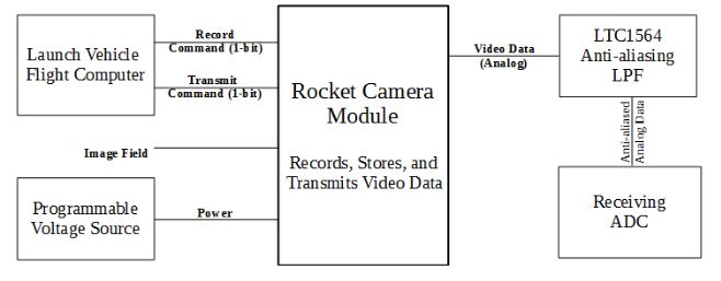
Figure I: Rocket Cam–level 0 Block Diagram
As its overall function, the design inputs light data, and then outputs an analog voltage representation of that data. The module also accepts two 1-bit command signals, the record and transmit commands, and it inputs power. Figure 1 shows this overall Level 0 functionality within the context of the larger rocket system, and Table III elaborates on each facet of it.
SYSTEM DESIGN-FUNCTIONAL DECOMPOSITION (Level 1)

Figure II: Rocket Cam–level 1 Hierarchical Decomposition
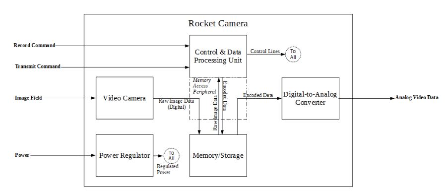
Figure III: Rocket Cam–level 1 Block Diagram
Figure II illustrates the primary sub-components of the module in hierarchical decomposition format. Figure III shows them in function structure format. In words, the control unit receives the Record and Transmit Commands from the outside world and controls the other sub-modules operations so that the device performs these tasks.
Upon receipt of the Record Command, the video camera activates, takes in visual data and outputs an uncompressed digital representation of this data, which the memory access peripheral routes into memory. The control & data processing unit then communicates with memory, in order to perform compression and encoding operations on the video data. The compressed and encoded version of the data gets stored back in memory.
TECHNOLOGY CHOICES AND DESIGN APPROACH ALTERNATIVES CONSIDERED
The primary technology choice central to this design, was how to implement the control/processing unit. Several possibilities were investigated. The two primary alternatives categories were: a low-cost ARM microcontroller with direct C programing and real time operation (typically targeted at controls applications), or a more expensive ARM microprocessor built for mobile applications and running a full operating system. Below are listed some of the pros and cons of each option.
PROJECT DESIGN DISCRETION
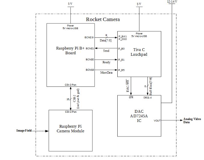
Figure V: Rocket Cam–implementation Concept Block Diagram Level 2
The Tiva C controls the AD7245A via a single-latched, parallel data loading structure (the AD7245A contains a double latched input, however, the design is configure so that one latch is left transparent). For simplicity the schematic wiring diagrams showing specific pinouts are broken into 3 diagrams, centered around the 3 main subcomponents. This prevents crossing wires in the diagrams. Signal names correspond to those shown in Figure V.

Figure VI: Ad7245a Pinout and Wiring Schematic
Figure VI shows the pin connections for the AD7245A DAC. The DAC is configured in unipolaR-mode, with the LDAC latch held transparent, the chip select engage, and latch clearing disabled. The design only makes use the upper 8 data bits and the lower 4 are tied to ground; this allows the design to make use of the higher precision the AD7245A has over most 8-bit DACs, without pushing the resolution to its limit and incurring less noise and drift resilience.
PHYSICAL CONSTRUCTION AND INTEGRATION
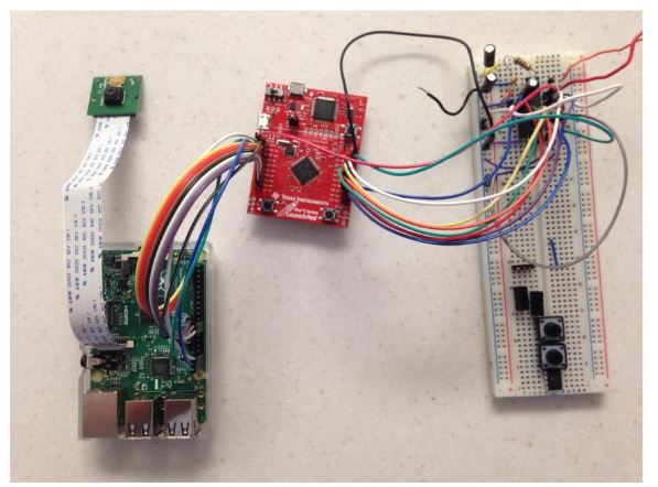
Figure Ix: Rocket Cam : Final Prototype
For prototyping purposes the design consists of the Tiva C Launchpad and Raspberry Pi B+ development boards, and an AD7245A in a PDIP package on a breadboard, all interconnected via wire-leads and jumpers, as shown in Figure IX.
INTEGRATED SYSTEM TESTS AND RESULTS
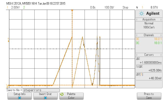
Figure XII: Oscilloscope Capture of Test Data Used to Determine Settling Error Threshold
The primary cause of unreadable bytes is parasitic RC delays that increase the settling time of large code transitions to the point that two settled sample values are not detected before the output transition to a new value. Using the test file whose analog output is shown in Figure XII, it was determined that at code transitions of greater than about 50, byte detection became unreliable.
CONCLUSIONS
The complete specifications were not met. Because of the noise and delay errors, the reconstructed, compressed video data file was corrupted and unreadable. In part this is due to the unforgiving nature of H264 compression, and compression in general, to errors. Compression involves the reduction of statistical redundancy in data, and reduction of redundancy also means a reduction in resilience to errors.
In its current state, the channel and reconstruction likely has sufficient accuracy for uncompressed video data to be sent and recovered with adequate quality. However, uncompressed video can not have the specified video duration and resolution and still be transmitted in the specified time. In addition, although documentation to the contrary exists, the drivers for the Raspberry Pi Camera Module do not currently support 30 frames per second capture, the videos are actually captured at 25 fps (83% the specified speed).
Despite its inability (in its current form) to meet all of the specifications simultaneously, this project serves as a solid proof of concept for the technology. In the trials discussed above, less than 0.2% of all bytes transmitted were unreadable, and of those that were readable almost all were within one least significant bit of the correct value. Moving forward with this project to a PCB design would most likely resolve the primary issues preventing the project from fully meeting all of the specifications.
A well designed PCB will have significantly lower parasitic capacitances than a breadboard circuit, allowing the time until a settled value, to be decreased, potentially to less than 100 μs for a full 10 V swing. Furthermore, implementation of noise suppression techniques and methods for isolating analog components from digital noise, should greatly reduce the number of least significant bit errors. This combined with improved reconstruction algorithms could potentially remove them altogether, allowing for complete, uncorrupted reconstruction of the compressed video data and achievement of all of the specifications.
Source: California Polytechnic State University
Authors: Thomas J. Higdon